100W Flyback Converter - Theory
100W Flyback Converter design and simulation.
Goals for this project:
Simulate a multi-output flyback converter capable of supplying 100W of power
Must Supply a well regulated output voltage of -24V at 4A
Must supply a 5V rail for digital logic
Use current mode control for the feedback loop
Output ripple must be less than 100mVpp
Input voltage range: 10V-30V
Switching frequency: 100kHz
Must Supply a well regulated output voltage of -24V at 4A
Must supply a 5V rail for digital logic
Use current mode control for the feedback loop
Output ripple must be less than 100mVpp
Input voltage range: 10V-30V
Switching frequency: 100kHz
Assumptions used for calculations:
Switching frequency of 100KHz
Nominal operating point at 50% duty ratio
Flyback transformer coupling coefficient: K = 0.99
Rectified wall voltage of 170V input
Max Vds of 450V for the switch * Based on power switches max breakdown
Assumption of 100% efficiency for base calculations
Nominal operating point at 50% duty ratio
Flyback transformer coupling coefficient: K = 0.99
Rectified wall voltage of 170V input
Max Vds of 450V for the switch * Based on power switches max breakdown
Assumption of 100% efficiency for base calculations
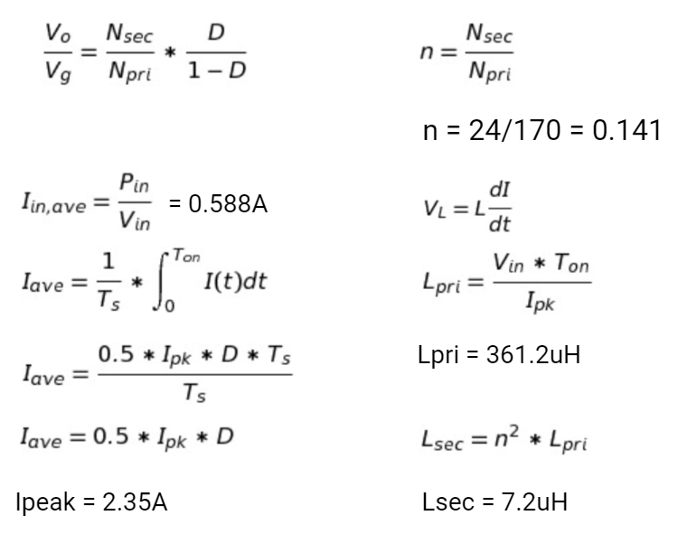
Calculations for the transformer:
Setting the duty cycle to 50% at the desired output voltage allows for the “n” turns ratio to be solved
Assuming 100% efficiency, the average input current is found
Using the average current the peak current is solved for
Now the primary inductance and secondary inductance can be found
Assuming 100% efficiency, the average input current is found
Using the average current the peak current is solved for
Now the primary inductance and secondary inductance can be found
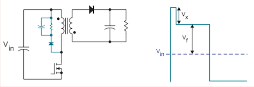
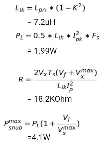
Snubber Design
To reduce the voltage spikes induced by the flyback transformer inductance, a snubber is needed
Reduced Vds to 450V from 2kV
Vx,max = 500V (Break down of switch)
Vf = Vo*n = Vin
Vx = 450V (desired overshoot)
Max loss of the snubber < 5% of the output power
Reduced Vds to 450V from 2kV
Vx,max = 500V (Break down of switch)
Vf = Vo*n = Vin
Vx = 450V (desired overshoot)
Max loss of the snubber < 5% of the output power
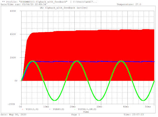
Simulation results settle at Vds = 450v as well
Red: Vds voltage
Blue: Rectified input
Green: AC input voltage
Red: Vds voltage
Blue: Rectified input
Green: AC input voltage
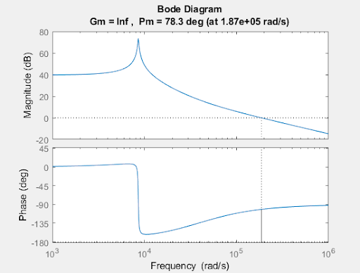
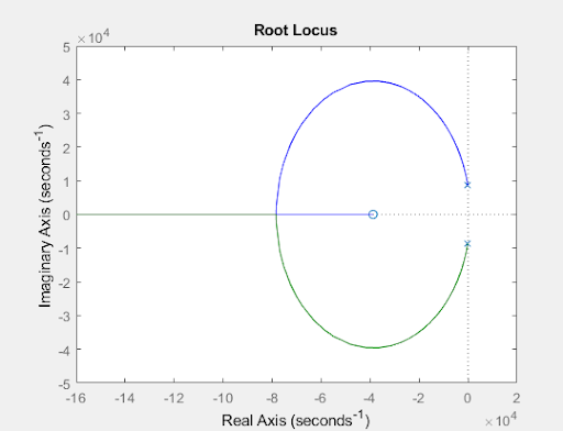
Stability Analysis
Control to output of the flyback converter meets the Ridley condition to move the LHZ to the right plane.
Stability Equation Rc*C > L/(D'*RL)
Rc = 0.03
RL = 12
C = 470uF
L = 7.225uH
Dp = 0.5
The condition is met:
L/(RL*Dp) = 1.2^(-6)
Rc*C = 1.41*10^(-5)
Rc*C > L/(RL*Dp)
Phase margin = 78.3Deg
Bandwidth = 30KHz
Stability Equation Rc*C > L/(D'*RL)
Rc = 0.03
RL = 12
C = 470uF
L = 7.225uH
Dp = 0.5
The condition is met:
L/(RL*Dp) = 1.2^(-6)
Rc*C = 1.41*10^(-5)
Rc*C > L/(RL*Dp)
Phase margin = 78.3Deg
Bandwidth = 30KHz
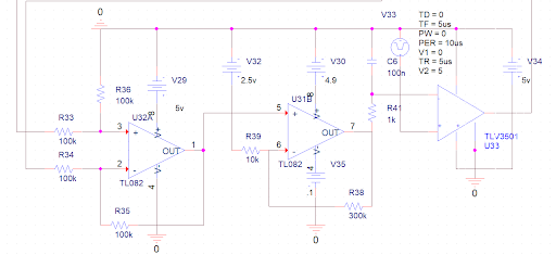
Feedback Circuit
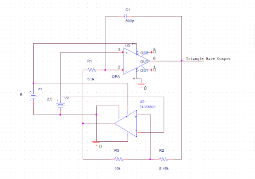
Triangle Wave Generator
Triangle wave generator using an operational amplifier and comparator.
Frequency can be found from:
R6 = 10KOhm
R5 = 8.45KOhm
R7 = 5.9KOhm
C3 = 500pF
Ft = 100KHz
Frequency can be found from:
R6 = 10KOhm
R5 = 8.45KOhm
R7 = 5.9KOhm
C3 = 500pF
Ft = 100KHz
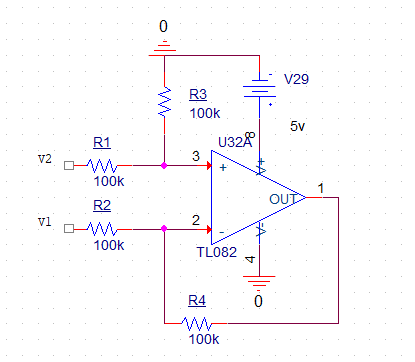
Error Amplifier
Using a differencing amplifier, the two error signals were added together
Transfer function of differencing amplifier: Vo=(R1/R2)(V2-V1)
By setting all the resistors to the same value, R1=R2=R3=R4 = 100kOhm and V1 as the negative output, the errors are added together with unity gain
Because Vref is set to 2.5V, each error signal must be set at 1.25V by voltage dividers
1.25/24 ratio
Ve = (1.25+E1-(-1.25-E2)) = 2.5+E1+E2
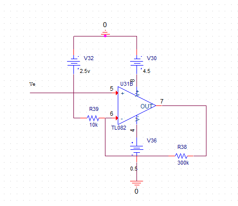
Proportional Control
Proportional control feedback loop used for output tracking
Proportional gain determined by R39 and R38
Gain of 30 gave quick response time and stable tracking
Voltage supplies set at 4.5V and 0.5V to prevent 0% and 100% duty cycle
Output to comparator to compare with Vref
Proportional gain determined by R39 and R38
Gain of 30 gave quick response time and stable tracking
Voltage supplies set at 4.5V and 0.5V to prevent 0% and 100% duty cycle
Output to comparator to compare with Vref
Comparator circuit with low pass filter to reduce noise
Low pass filter set at 10KHz to filter out switching frequency noise
13dB attenuation at 100Khz
TLV3501 comparator for high speed switch to gate driver
Had good response with no filter, but the error signal had lots of noise
Low pass filter set at 10KHz to filter out switching frequency noise
13dB attenuation at 100Khz
TLV3501 comparator for high speed switch to gate driver
Had good response with no filter, but the error signal had lots of noise
Simulation Results
Feedback circuit without the low pass filter
Green: Error voltage before proportional amplifier
Yellow: Error with just proportional increase
Green: Error voltage before proportional amplifier
Yellow: Error with just proportional increase
Pink: Error signal
Blue: Amplified error signal
Red: Triangle wave
Green: PWM output from comparator
Blue: Amplified error signal
Red: Triangle wave
Green: PWM output from comparator
Flyback with Feedback Schematic.
Voltage dividers of 18.2KΩ and 1KΩ to set error signals large signal voltage to 1.25V
Vm = 5v
Vref = 2.5v
Vcc = 5v
Ve = 2.5+E1+E2
Voltage dividers of 18.2KΩ and 1KΩ to set error signals large signal voltage to 1.25V
Vm = 5v
Vref = 2.5v
Vcc = 5v
Ve = 2.5+E1+E2
Output voltages using the full bridge rectifier
Maximum load of 100W
No overshoot with full bridge rectifier circuit
No low pass filter at error amplifier stage
Maximum load of 100W
No overshoot with full bridge rectifier circuit
No low pass filter at error amplifier stage
References / Resources
PWM and triangle wave generator example:
http://www.ti.com/lit/an/sboa212a/sboa212a.pdf
Inductive coupling in pspice:
https://www.pspice.com/resources/application-notes/using-inductor-coupling-symbols
R. Ridley snubber design for flyback:
http://cdn14.21dianyuan.com/download.php?id=82185
5 Loop Gain Analysis of switching converters
https://ieeexplore-ieee-org.libproxy.utdallas.edu/document/678481
R. Ridley elimination of positive zero in flyback:
https://ieeexplore.ieee.org/stamp/stamp.jsp?tp=&arnumber=66413
R. Ridley Compensation methods:
https://www.researchgate.net/publication/280308828_Designing_with_the_TL431_-_the_first_complete_analysis
Compensation methods:
https://www.onsemi.com/pub/Collateral/TND381-D.PDF
← Back to Home
http://www.ti.com/lit/an/sboa212a/sboa212a.pdf
Inductive coupling in pspice:
https://www.pspice.com/resources/application-notes/using-inductor-coupling-symbols
R. Ridley snubber design for flyback:
http://cdn14.21dianyuan.com/download.php?id=82185
5 Loop Gain Analysis of switching converters
https://ieeexplore-ieee-org.libproxy.utdallas.edu/document/678481
R. Ridley elimination of positive zero in flyback:
https://ieeexplore.ieee.org/stamp/stamp.jsp?tp=&arnumber=66413
R. Ridley Compensation methods:
https://www.researchgate.net/publication/280308828_Designing_with_the_TL431_-_the_first_complete_analysis
Compensation methods:
https://www.onsemi.com/pub/Collateral/TND381-D.PDF